Time: 2024-08-20
Chip manufacturing has always been a challenge due to the complexity of ensuring that billions of interconnected transistors are defect - free . However , researchers at the Paul Scherrer Institute in Switzerland and the USC Viterbi School of Engineering have developed a groundbreaking 3D imaging technique using X - rays to detect any alterations in computer chips . This non - destructive method allows for efficient identification of subtle manufacturing defects , enhancing hardware security significantly.
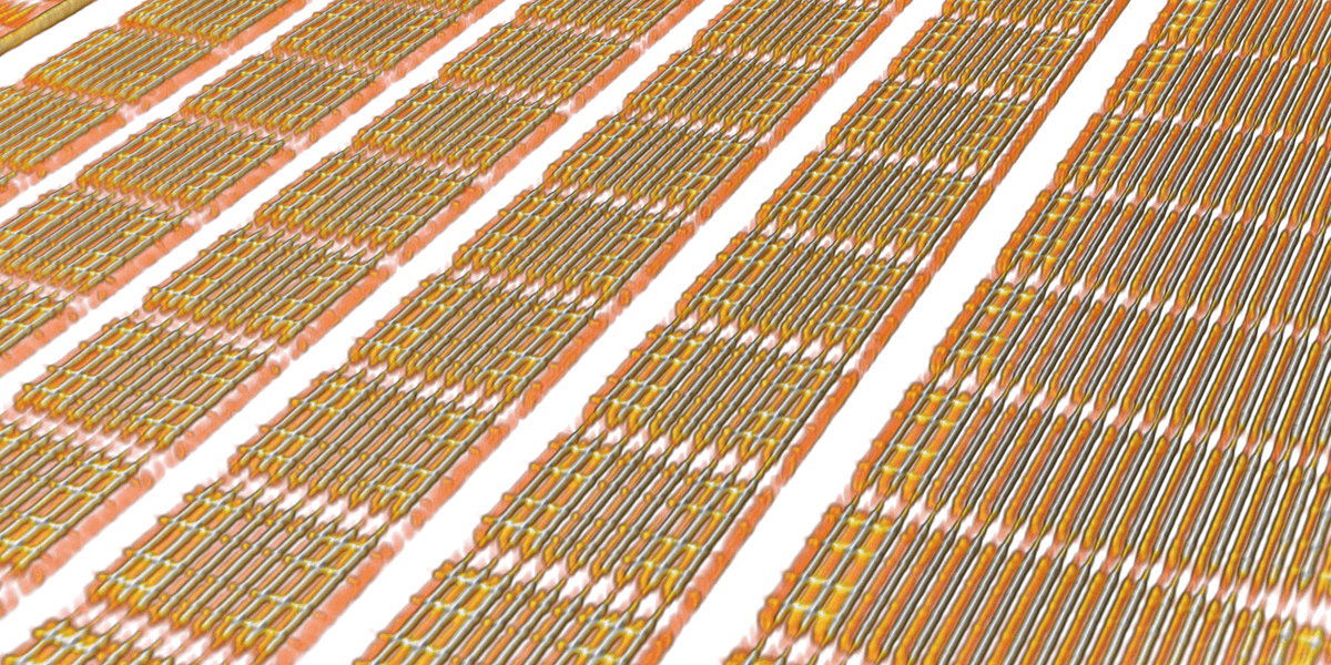
By utilizing ptychographic X - ray laminography , the team was able to illuminate small regions of rotating chips with X - rays at a specific angle to generate high - resolution slice images . These images are then used to create detailed 3D renderings of the chip interiors , providing a means for comparison with the original design . This innovative approach ensures that chips are manufactured accurately and meet design specifications , offering a new level of quality assurance in chip production.
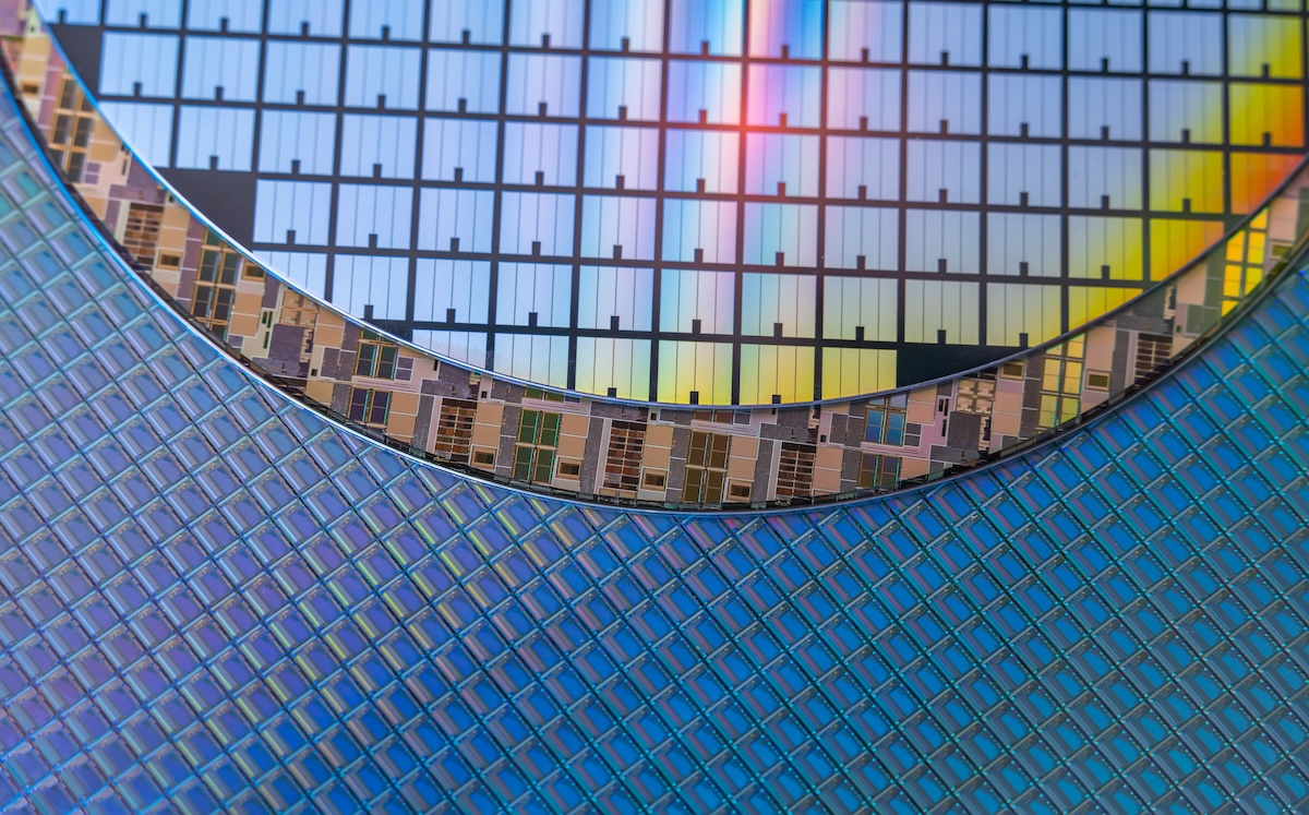
The new method allows for the validation of the integrity of computer chips at an unprecedented level of detail , with a remarkable 4 nm resolution . By reducing mechanical vibrations and improving imaging algorithms , the team has achieved a 10x increase in depth of field and a much faster acquisition rate . This advancement opens up possibilities for future 3D imaging of chips with sub - nm resolution , non - destructive reverse engineering of integrated circuits , and chip manufacturing services.
In a separate study , researchers from Tufts University and Istituto Italiano di Tecnologia have developed a novel chip nanomanufacturing approach that uses water as the primary solvent , minimizing the need for toxic chemicals . By incorporating silk protein into water , the researchers were able to enhance its ability to evenly cover various surfaces , making it suitable for depositing water - soluble materials and metals on silicon and polymers with nanometer precision.
This environmentally friendly approach not only offers a safer alternative to traditional chip manufacturing processes but also demonstrates compatibility with a wide range of materials , including indium gallium zinc oxide transistors , aluminum oxide insulators , and perovskite films . The method 's versatility and ease of integration into existing manufacturing processes make it a promising solution for the future of chip production .
By combining cutting - edge X - ray imaging techniques for chip analysis with innovative water - based solvents for chip nanomanufacturing , researchers are pushing the boundaries of technology and paving the way for advancements in the field of integrated circuits . These developments offer a glimpse into a future where chips are not only more secure and reliable but also produced in a more sustainable and environmentally friendly manner.


 Business
